8. Electron Diffraction
8.1. Background
In 1923, in his doctoral dissertation, Louis de Broglie proposed that all forms of matter have wave as well as particle properties, just like light. The wavelength, \(\lambda\), of a particle, such as an electron, is related to its momentum, \(p\), by the same relationship as for a photon:
where \(h\) is Planck’s constant. The wave properties of electrons are illustrated in this experiment by the interference, which results when they are scattered from successive planes of atoms in a target composed of graphite micro crystals. The spacing between successive planes is obtainable from the interference pattern.
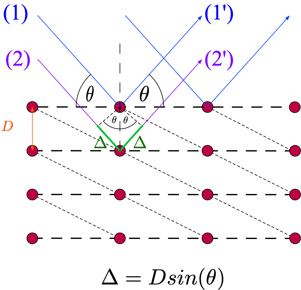
Fig. 8.1 Reflection of electron waves from atomic planes. Ray 1 and 2 have no path length difference, \(2 \Delta\) is the path length difference between ray 1 from the top plane and ray 3 from the one below. The short-dashed lines show another possible set of atomic planes.
A useful model for the formation of diffraction pattern in X-ray diffraction is due to W.H and W.L Bragg (1913). They regarded the crystal to me made of parallel (atomic) planes from which the X-ray or electron waves are reflected specularly (incident angle equal reflected angle). Only a small fraction of the wave is reflected from each plane and the final superposition of these reflected waves lead to the observed diffraction pattern. For a single crystal, strong reflection of waves occurs when the so-called Bragg condition is met:
Which is the same as the one for X-ray diffraction (see the explanation there). Here \(\lambda\) is electron matter wave length, \(\theta\) is the incident angle and \(d\) is the distance between the atomic planes.
In the graphite target, there are very many perfect micro crystals randomly oriented to one another.
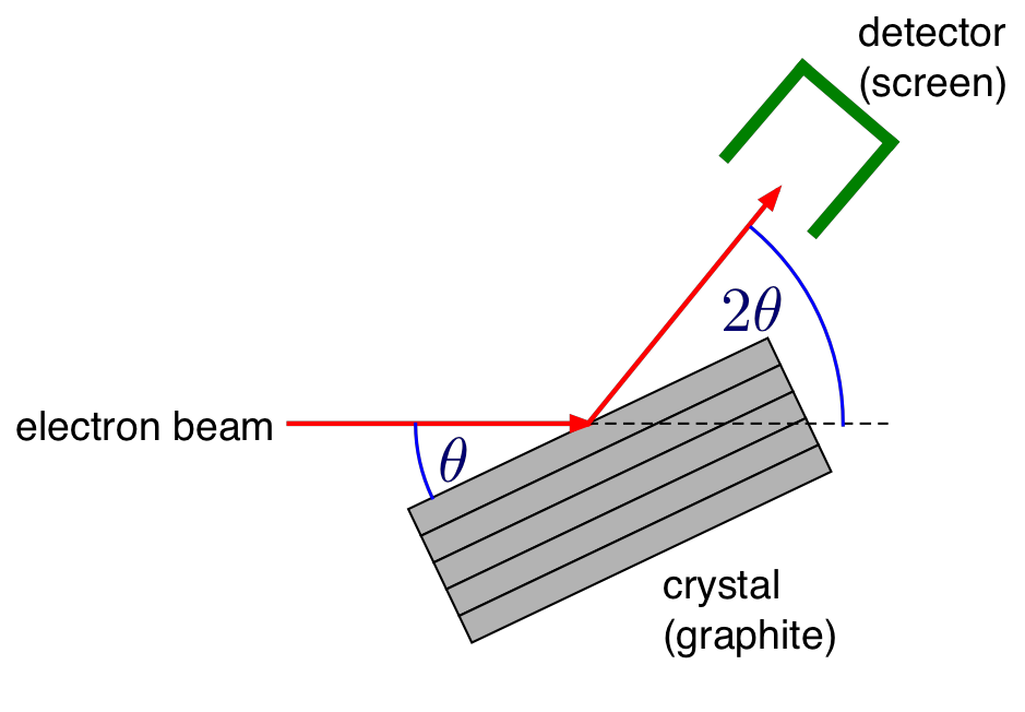
Fig. 8.2 Geometry for diffraction from a single graphite crystal
Therefore the strongly emerging beam will be of a conical shape of half-angle \(2\theta\) as shown in Fig. 8.3. If this beam falls on a phosphor-coated screen, rings of light will be formed.
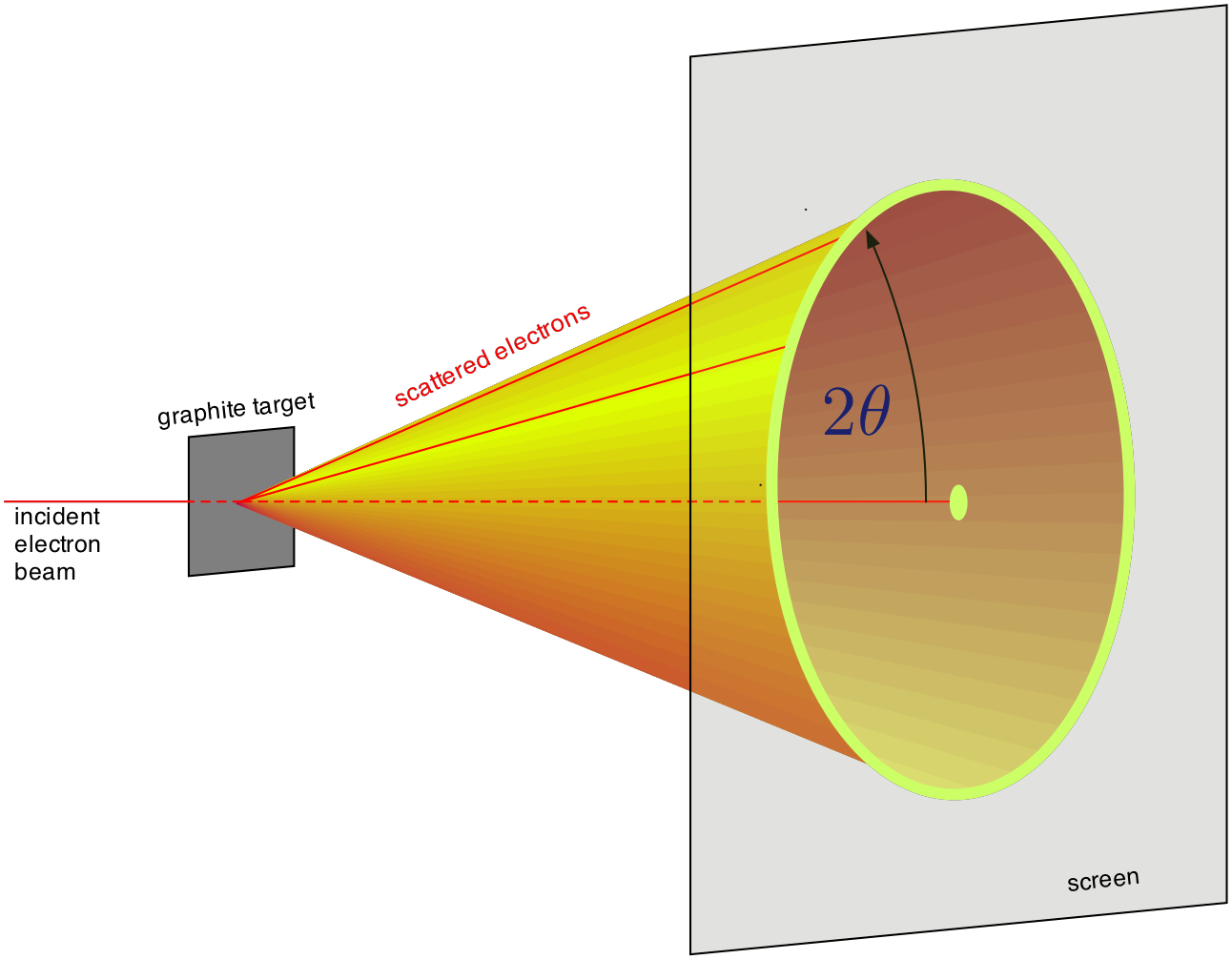
Fig. 8.3 Diffraction from a large number of micro crystals
8.2. Experimental Setup
The apparatus is shown in Fig. 8.4. Electrons emitted by thermionic emission from a heated filament (4) inside the cathode are accelerated towards the graphite target (9) of the anode by a potential difference, \(V_a\) between the cathode and anode. A focusing electrode (8) is located in front of the target to focus the electron beam in order to provide a sharp interference pattern on the screen (11).
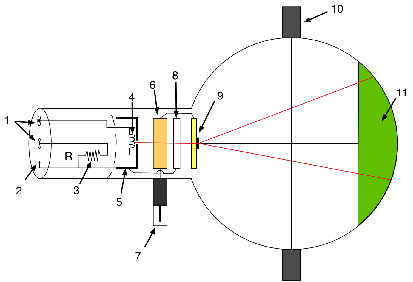
Fig. 8.4 Overview of the electron diffraction tube.(1)4-mm socket for filament heating supply, (2) 2-mm socket for cathode connection, (3) internal resistor, (4) filament. (5) cathode, (6) anode, (7) 4-mm plug for anode connection (HV), (8) focusing electrode, (9) polycrystalline graphite grating, (10) Boss, (11) fluorescent screen.
Their kinetic energy, \(K\), on reaching the target is equal to their loss of potential energy:
from equations (8.1) and (8.3) one obtains:
8.3. Experimental Procedure
Connect the power supplies, a historic HV voltmeter (for high voltage (HV) measurements) and a micro-ammeter to the vacuum tube as shown in Fig. 8.5
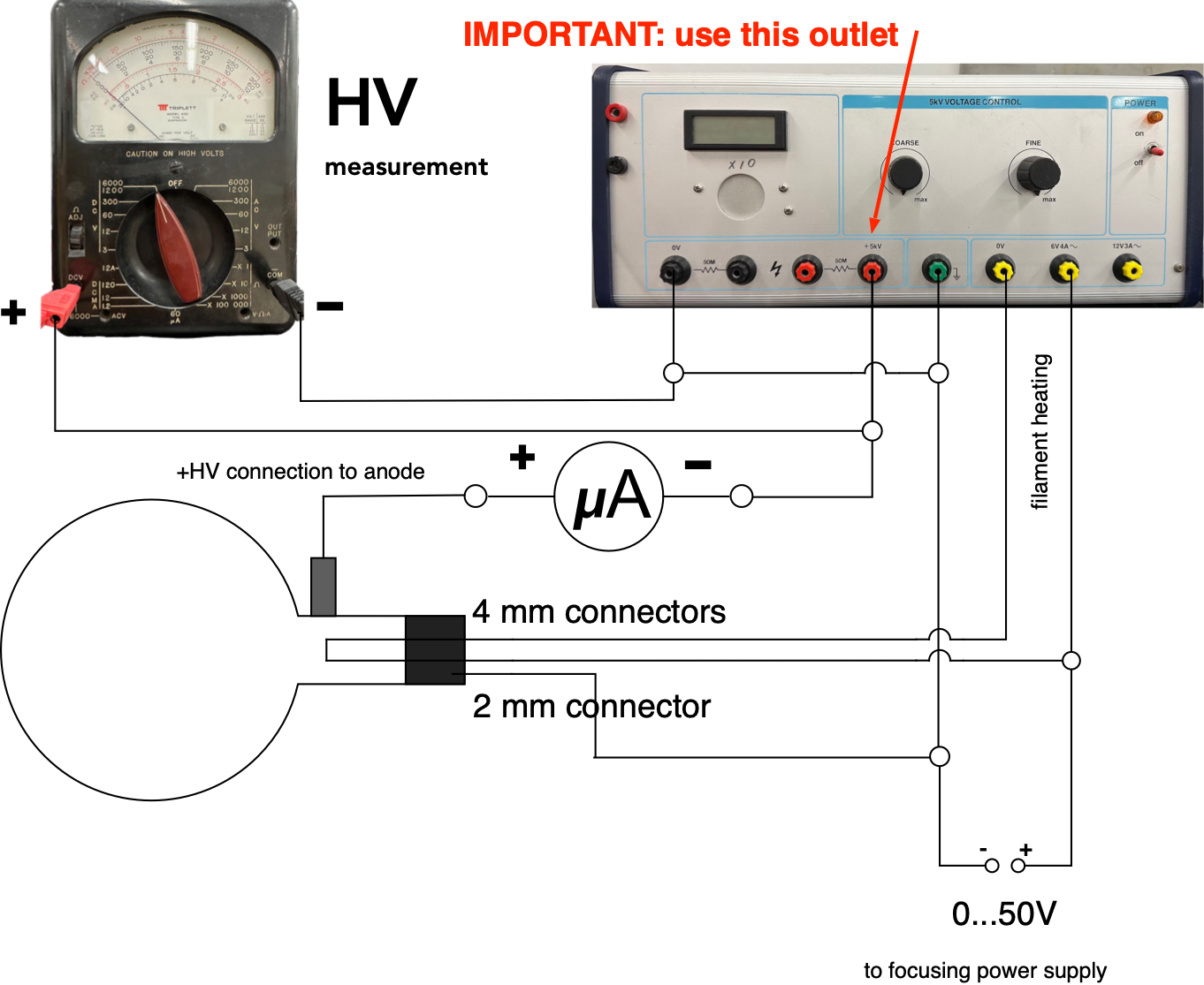
Fig. 8.5 Connecting the electron diffraction tube
HAVE THE CIRCUIT CHECKED BY YOUR INSTRUCTOR BEFORE TURNING ANYTHING ON.
The use the historic volmeter to measure the acceleration voltage Adjust the voltage controls on the power supplies to zero and then turn them on. Wait a few minutes for the filament to warm up. Set the focusing/intensity voltage to around 10 - 15 V and then slowly increase the accelerating voltage to 3 kV. A bright central spot and two rings should be observable on the screen. The rings are due to first order (n = 1) diffraction from two different sets of atomic planes having different spacings. Adjust the focusing/intensity voltage until the rings are as sharply defined as possible and then measure their diameters. Try to find a setting that produces the best images for the lowest accelerating voltage, where the rings are barely visible (about 1.5 kV) , as well as the highest accelerating voltage \(V_a\) (about 4kV) Obtain measurements for 5 - 6 different accelerating voltages, \(V_a\), over as wide a range as possible.
Use the IDS camera to take pictures of the rings. Determine the ring diameters and their uncertainties from the images using the ImageAnalyzer. For help ask an instructor.
8.4. Analysis
The geometry for the vacuum tube is shown in Fig. 8.6.
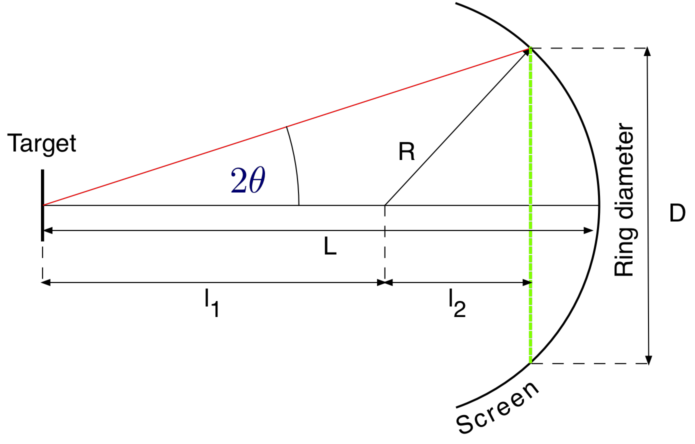
Fig. 8.6 Vacuum tube geometry
The value of \(\theta\) can be obtained from
here \(R = 6.25\ cm\) and \(L = 13.7\ cm\). The structure of graphite is shown in Fig. 8.7. The two possible layers are indicated by dashed lines.
Using the ImageAnalyzer and the calibration image to determine the image scale needed to determine the ring diameters (see ImageAnalyzer )
The most effective way to determine the ring diameters in each image is to determine the location of the ring edges from left to right as shown in Fig. 8.8. Write a function that returns the two ring diameters and their uncertainties and uses the the data file name as argument. (hint: you can calculate derivatives numerically see the Collection of useful tools
Write a function that calculates the atomic plane separation including its uncertainty based on equations (8.5), (8.4) and (8.2).
Make a plot of your result as a function of the voltages. Include all error bars. Determine the weighted average values and their uncertainties.
From your measured data determine the distance \(s\) between the carbon atoms and compare your result to the value provided in Fig. 8.7. Does it agree within your error bars, if not how big is the deviation in units of your error bar?
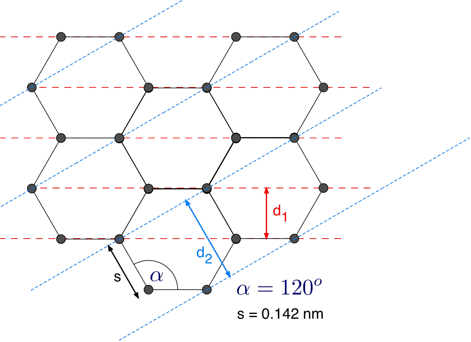
Fig. 8.7 The structure of graphite with Bragg planes.
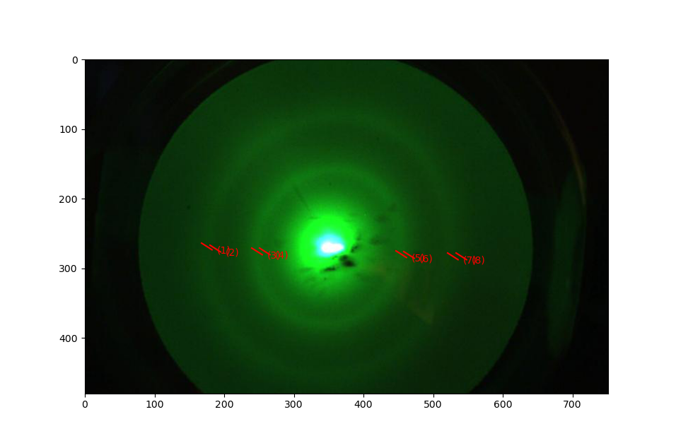
Fig. 8.8 Determination of the locations of the diffraction ring edges from left to right. From these data the ring diameters and their uncertainties can be determined.